- Have you ever seen a green board inside a mobile phone, remote control, or any electronic devices?
- This board helps all the electronic parts work together.
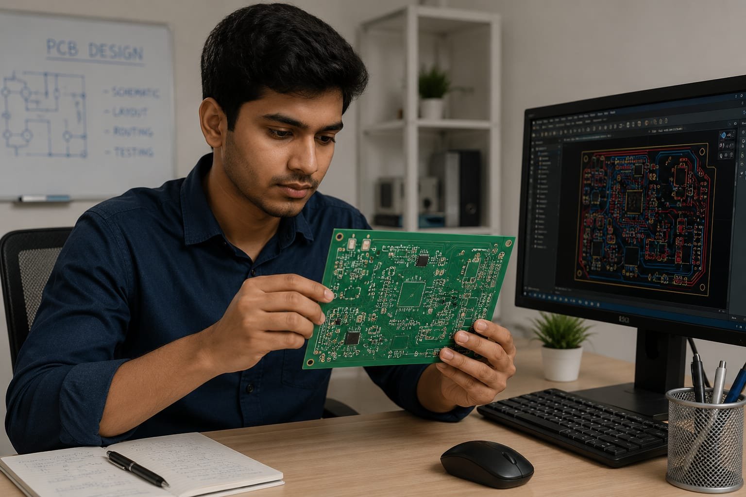
- This green board is called a Printed Circuit Board (PCB).
- The person who designs these boards is called a PCB Design Engineer.
- 👉 In simple words: PCB Design Engineers design the circuit boards used inside electronic devices.
PCB Design Engineer
What Do They Do?
🎓 How to Become a PCB Design Engineer
You have two options:
-
Start early with a Diploma
After Class 10, you can choose a relevant diploma course. Complete the diploma and join the second year of an engineering course by applying through lateral entry. -
Finish Class 12
Complete Class 11 and 12, then you can do a B.Tech./B.E. in the relevant field.
These beginner-level courses help students learn electronics, circuit design, PCB fundamentals, electronic components, and hardware design basics.
Diploma in Electronics Engineering
Duration: 3 Years
Eligibility: Class 10 Pass
Entrance Exam: Polytechnic Entrance Exam / Merit-Based Admission
Diploma in Electronics and Communication Engineering (ECE)
Duration: 3 Years
Eligibility: Class 10 Pass
Entrance Exam: Polytechnic Entrance Exam / Merit-Based Admission
📝 Exam Details
(Click on the exam name to see full details)
Polytechnic Entrance Exam Merit-Based AdmissionNote: A diploma teaches circuit testing, soldering, and PCB fundamentals. However, advanced PCB design roles usually require a Bachelor's degree or specialized PCB design certifications.
These degree programs help students learn electronic systems, circuit design, embedded hardware, PCB development, and modern electronics engineering.
B.Tech / B.E. in Electronics and Communication Engineering (ECE)
Duration: 4 Years
Eligibility: 10+2 Pass with PCM
Entrance Exam: JEE Main / State Engineering Entrance Exams
B.Tech / B.E. in Electronics Engineering
Duration: 4 Years
Eligibility: 10+2 Pass with PCM
Entrance Exam: JEE Main / State Engineering Entrance Exams
📝 Exam Details
(Click on the exam name to see full details)
JEE Main State Engineering Entrance ExamsNote: To become a PCB Design Engineer, students should also learn industry PCB design software such as Altium Designer, KiCad, OrCAD, or Eagle through practical projects.
Diploma holders can directly enter the second year of selected engineering degree programs through lateral entry admissions.
B.Tech Lateral Entry in Electronics & Communication Engineering
Duration: 3 Years
Eligibility: Diploma in Electronics-related Branches
Entrance Exam: State Lateral Entry Entrance Tests
B.Tech Lateral Entry in Electronics Engineering
Duration: 3 Years
Eligibility: Diploma in Electronics-related Branches
Entrance Exam: State Lateral Entry Exams
These advanced programs help engineers specialize in electronics system design, hardware development, and professional PCB design technologies.
M.Tech in Electronics Product Design (EPD)
Duration: 2 Years
Eligibility: B.Tech / B.E. in Electronics-related Branches
Entrance Exam: GATE / University PG Exams
Note: Advanced PCB design engineers often specialize in high-speed PCB design, signal integrity, hardware architecture, and electronic product development.
Note:
(Age limits, marks, and admission process may vary depending on the college or state.
Below are some colleges that offer these courses.
These courses are available in many colleges and universities across India. You can choose colleges based on your location, budget, and entrance exams.)
🏛️ Colleges offering these courses in India
(Tap on a college to visit the official website)
After Class 12
Manipal Institute of Technology (MIT), Manipal Manipal Institute of Technology (MIT), Manipal M.S.Ramaiah University of Aaplied Sciences, Bengaluru, KarnatakaSTEP 1
Imagine you are working as a PCB Design Engineer.
STEP 2
Your company is making a new smartwatch.
STEP 3
The smartwatch needs a PCB to connect all its electronic parts.
STEP 4
Your job is to design the PCB.
STEP 5
You decide where all the electronic parts should be placed.
STEP 6
Using your design, the PCB is made in a factory.
STEP 7
If you enjoy electronics, design, and creating technology products, this career may be right for you.
Where do PCB Design Engineers work? (Job Roles + Growth)
PCB Design Engineers work in : Electronics companies, Semiconductor companies, Consumer electronics companies, Automotive companies, Aerospace companies, Medical device companies, Telecommunications companies, and Industrial automation companies.
🟢 Beginner Roles
Junior PCB Layout Engineer
(0–2 Years Experience)
Designs basic PCB layouts using CAD software.
Hardware Test Engineer
(0–2 Years Experience)
Tests circuit boards and finds hardware issues.
🔵 Mid-Level Roles
PCB Design Engineer
(2–5 Years Experience)
Designs complex multi-layer circuit boards.
Hardware Design Engineer
(3–5 Years Experience)
Creates circuit designs for electronic products.
🟣 Advanced Roles
Senior Hardware Architect
(5+ Years Experience)
Designs advanced electronic systems and boards.
VP of Hardware Systems
(8+ Years Experience)
Leads teams developing electronic products.
Consumer Electronics Companies
Design PCBs for smartphones, laptops, and smart devices.
Automotive Technology Companies
Create PCBs used in modern vehicles and EVs.
Industrial Automation Companies
Design circuit boards for machines and factories.
Medical Equipment Companies
Develop PCBs for medical devices and equipment.
Aerospace & Defense Organizations
Build PCBs for aircraft, satellites, and defense systems.
Electronics Research Organizations
Create advanced PCB technologies for future products.
(Click Yes or No for each question)
1. When you opened a mobile phone or remote control, have you seen a green-colored board inside it?
2. Do you know what this green board does inside an electronic device?
3. Would you like to learn how engineers design these green circuit boards?
4. Imagine you are working as a PCB Design Engineer for a company that makes smartphones. Every smartphone has a green circuit board that connects its electronic components. Your job is to design this board and decide where the components and connections should go. Would you enjoy doing this kind of work?
5. Imagine a company is making a new smartwatch. Your job is to design the green circuit board inside it. The board you designed helps the smartwatch work properly. Does this sound exciting to you?